
I think this forum is still lacking a definite thread for guidelines designing a BMS, whether commercial or just DIY for one's own use.
I was replying to http://www.diyelectriccar.com/forum...s/showthread.php/estimate-bms-cost-per-lithium-batteryi-p339260.html#post339260 but thought it would be off-topic, hence this new thread. So here's what I was going to reply...
BMS is simple as hell. Don't overengineer it.
IMHO, think about redistributive balancing only if you are going to mix variety of cells with varying specifications or quality.
Do a careful top-balance manually; let the BMS shunting take care of minor imbalance caused by self discharge and peukert effects, which are both almost nonexistent in all li-ion.
Recovering shunting energy is easy, I have built some prototypes (of bi-directional flyback transformer construction), but still, the amount of energy wasted there is so tiny... Does it make sense to do active balancing when using new, identical li-ion cells?
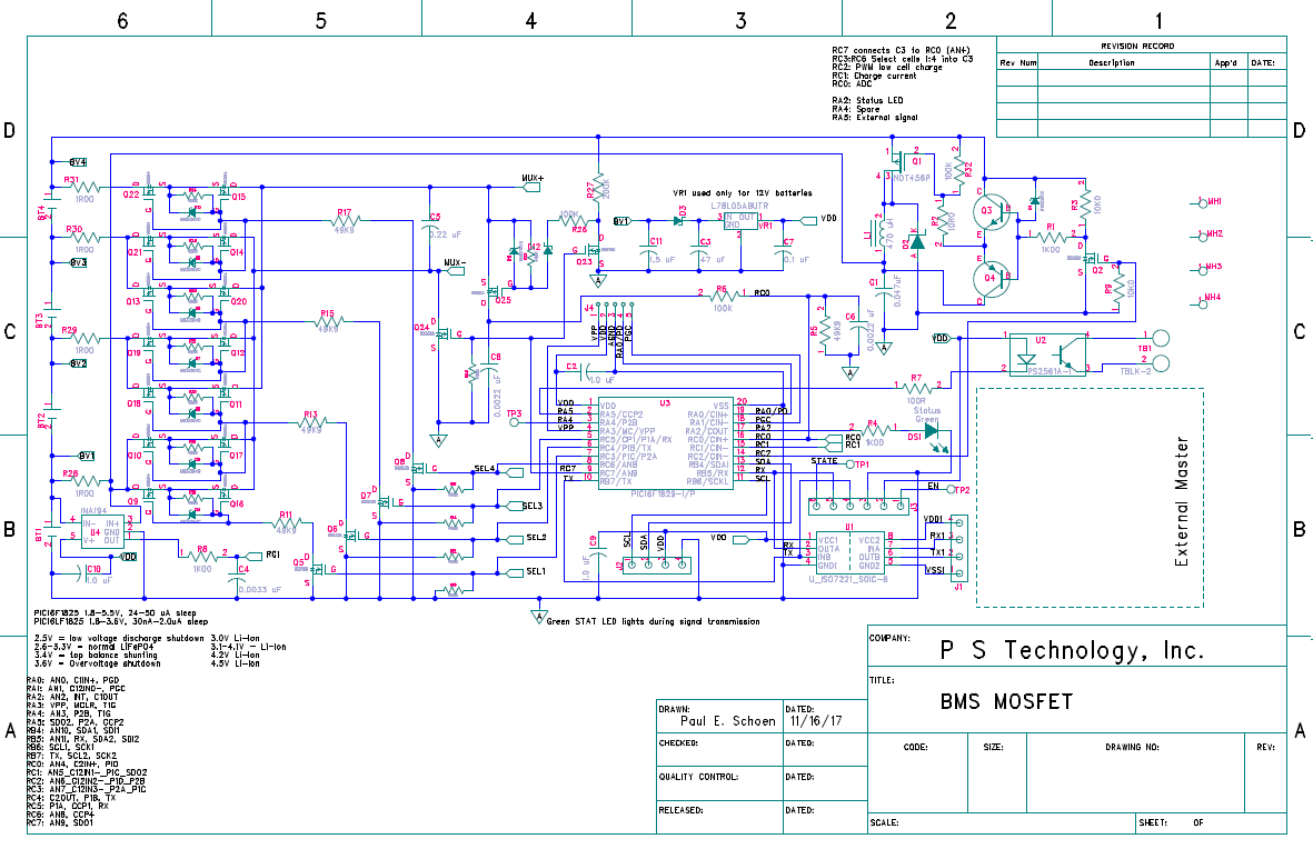
I would consider pointing all design efforts towards reliability, and key to reliability is in simplicity and careful consideration of all possible use & misuse cases. Look at the MiniBMS; they have a long thread on this forum where they share the schematic. It's important to take a look at how they solve design challenges for maximum simplicity, reliability and minimum cost in mind.
IMO, one MCU per cell is a good idea. Pick an MCU that has an integrated temperature sensor and you get an extra feature for free.
Implement:
- Low voltage shutdown for motor controller
- High voltage shutdown for charger
- Low voltage shutdown for charger (do not allow charging damaged cells). This is especially important for LiCoO2.
- High temperature shutdown for both motor & charger
- Low temperature charging disable/limiter (jeffcoat)
- Error & statistics reporting
Also:
- Make sure that no error condition such as
- full battery pack voltage over the cell module terminals
- short circuit on cell module
would cause excessive heat on the module,
- Make sure ALL error conditions cause shutdown for motor controller and charger.
- Add DC rated fuse
- make sure that it will blow before the shunt MOSFET & resistor get too hot in case of latch-on fault.
- For any problem you are going to solve by adding a new feature, make sure this problem really exists, measure and analyze it.
I'm thinking about compiling a small guide or "FAQ" on BMS design points. So any additions to this list are very welcome. I'll start by editing this list to add new points.
I was replying to http://www.diyelectriccar.com/forum...s/showthread.php/estimate-bms-cost-per-lithium-batteryi-p339260.html#post339260 but thought it would be off-topic, hence this new thread. So here's what I was going to reply...
BMS is simple as hell. Don't overengineer it.
IMHO, think about redistributive balancing only if you are going to mix variety of cells with varying specifications or quality.
Do a careful top-balance manually; let the BMS shunting take care of minor imbalance caused by self discharge and peukert effects, which are both almost nonexistent in all li-ion.
Recovering shunting energy is easy, I have built some prototypes (of bi-directional flyback transformer construction), but still, the amount of energy wasted there is so tiny... Does it make sense to do active balancing when using new, identical li-ion cells?
I would consider pointing all design efforts towards reliability, and key to reliability is in simplicity and careful consideration of all possible use & misuse cases. Look at the MiniBMS; they have a long thread on this forum where they share the schematic. It's important to take a look at how they solve design challenges for maximum simplicity, reliability and minimum cost in mind.
IMO, one MCU per cell is a good idea. Pick an MCU that has an integrated temperature sensor and you get an extra feature for free.
Implement:
- Low voltage shutdown for motor controller
- High voltage shutdown for charger
- Low voltage shutdown for charger (do not allow charging damaged cells). This is especially important for LiCoO2.
- High temperature shutdown for both motor & charger
- Low temperature charging disable/limiter (jeffcoat)
- Error & statistics reporting
Also:
- Make sure that no error condition such as
- full battery pack voltage over the cell module terminals
- short circuit on cell module
would cause excessive heat on the module,
- Make sure ALL error conditions cause shutdown for motor controller and charger.
- Add DC rated fuse
- make sure that it will blow before the shunt MOSFET & resistor get too hot in case of latch-on fault.
- For any problem you are going to solve by adding a new feature, make sure this problem really exists, measure and analyze it.
I'm thinking about compiling a small guide or "FAQ" on BMS design points. So any additions to this list are very welcome. I'll start by editing this list to add new points.
") . with each slave translating the voltage.
. with each slave translating the voltage.